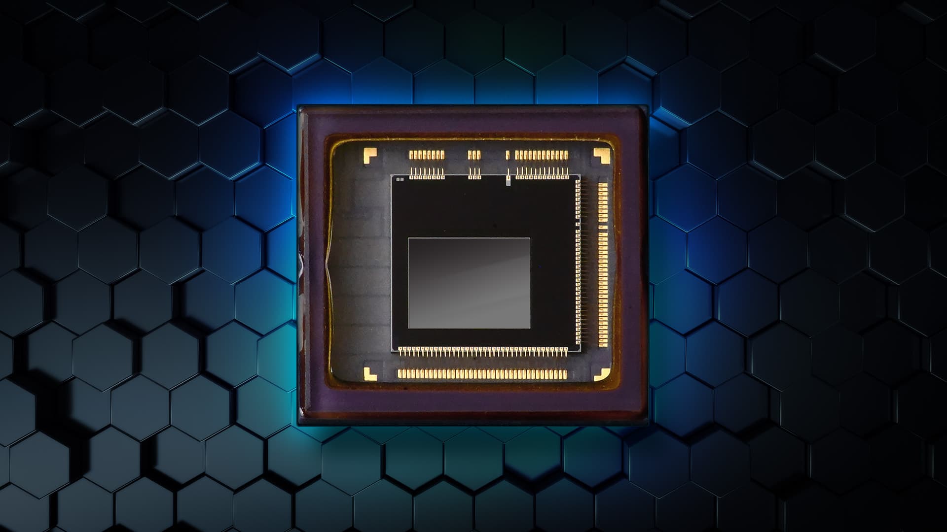
FRAMOS has introduced a ToF camera development kit for vision system engineers who are investigating Time-of-Flight technology, or who are working to develop ToF cameras for machine vision applications. When we set out to create a development kit and camera module for evaluating Time-of-Flight technology, we determined to build it around the most performant indirect Time-of-Flight (iToF) image sensor we could find.
We ended up selecting Sony Semiconductor Solutions new IMX570 ToF sensor. The sensor is positioned to become the industry leading sensor for a wide range of embedded vision applications. Here’s why:
Back-Side Illumination Technology
Like many of Sony’s next-generation CMOS sensor products, the IMX570 was developed using back-side illumination (BSI) technology.
One of the challenges in reducing the pixel size of CMOS sensors stems from the fact that in standard sensor designs, the chip wiring and other components have to be overlaid on top of the active matrix of photosensitive material. This requires the addition of microlenses to direct light between the upper elements of the chip, and restricts the degree to which the pixels can be miniaturized without a corresponding loss of sensitivity.
This can be overcome to a degree by increasing the gain of the sensor, but this is always a trade off, as this results in increased signal noise as the sensor density increases.
Back-side illumination architecture eliminates this problem by inverting the structure of the sensor, and effectively moving the wiring from the top to the bottom of the sensor. This is accomplished by carefully polishing the back-surface of the wafer to allow light to reach the sensitized active matrix of the sensor.
BSI architecture requires nanometer precision polishing and advanced manufacturing methods, but the result is a net increase in sensitivity to low light with lower noise and while allowing the development of denser, higher resolution sensors with a smaller footprint.
5 Micrometer Pixel Architecture
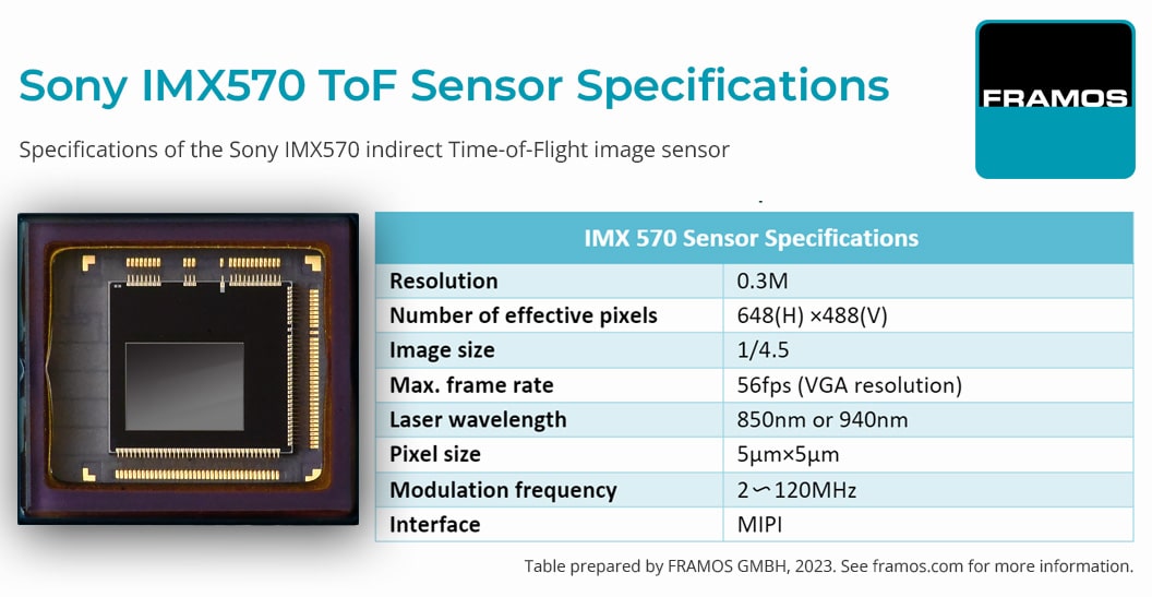
The IMX570 image sensor features 5 micrometer pixel architecture, resulting in smaller sensor dimensions. The sensor size is only 1 / 4.5”, allowing the construction of more compact cameras using smaller optics.
The sensor’s small size means that it’s ideal for embedded vision applications where a small camera footprint is desirable.
High Resolution ToF Sensing
The IMX570 sensor is 644 by 488 pixels, and delivers an effective resolution of 640×480 (VGA) resolution.
While this may seem like a modest resolution when compared to image sensors for ordinary visible light cameras, this is higher resolution that is available in most Time-of-Flight image sensors and provides a degree of fidelity previously unavailable in Time-of-Flight cameras.
The high resolution and fidelity of this sensor make it a good choice for robotics and object recognition applications.
High Operating Speed
The IMX570 sensor operates at up to 56 frames per second, reducing image blurring of moving objects, and making it an ideal choice for real-time applications.
However, it should be noted that the ToF camera module in our development kit has been capped at 30 frames per second for thermal management reasons. This is because the development kit is provided with a high-output illumination board, equipped with four 1-watt VCSEL (Vertical Cavity Surface-Emitting Laser) laser emitters.
If you are interested in evaluating the IMX570 ToF sensor at higher frame rates, our engineers can work with you to modify the illumination board and sensor module in our development kit to run at lower power levels.
Robust Under Varied Lighting Conditions
Since Time-of-Flight cameras are an active sensing technology that provides its own illumination, they tend to work well indoors or in low light conditions, but they tend to be less effective outdoors or in bright conditions where the laser illumination can be washed out by ambient light sources.
The IMX570 sensor features a “pixel drive” processing circuit to reduce the effects of unwanted ambient light. This improves accuracy of the sensor in highly illuminated environments or outdoors under bright sunshine. The IMX570 sensor is also effective in dark environments, such as an unlit warehouse.
Robust Feature Set
The IMX570 includes a robust feature set, which is useful when developing application software for a new ToF camera.
We have exposed access to complex sensor features in the software and drivers provided with our Time-of-Flight development kit, including access to the raw sensor data.
Evaluate the IMX570 For Yourself
If you are interested in evaluating Time-of-Flight technology for a new application, or have a camera development project in mind, the FRAMOS FSM-IMX570 development kit can provide you with an easy way to experiment with Sony’s ToF technology, or to develop your own prototype camera system.
The development kit provides vision system engineers with a simple, coherent framework for quickly developing a working prototype of an indirect Time-of-Flight (iToF) camera system based on Sony’s industry-leading iToF technology. The kit includes a calibrated camera module and is designed to interface with NVIDIA Jetson family of System-on-Module embedded computers, including Jetson Xavier and Orin series SoMs.
To learn more about the FSM-IMX570 development kit, you can view the product specifications.


