Visible, NIR, and SWIR Wavelengths
One of the new and exciting areas that is showing a lot of promise for industrial applications is the use of Near and Short Wavelength Infrared (NIR and SWIR) light to gather information that is not visible to the human eye. Many times, the information gathered in these wavelengths augment the data seen in the visible, 350-750 nm, spectrum. NIR wavelengths are in the range of 780-1400 nm while SWIR is in the range of 900–2500 nm.
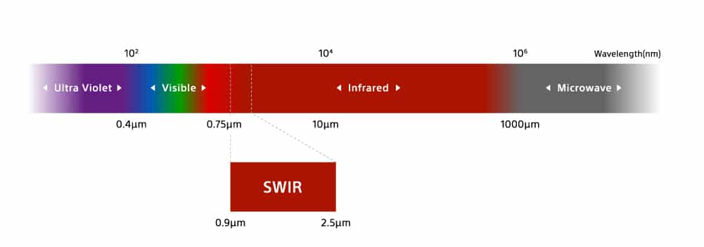
Though NIR light has been used extensively in many machine vision applications, many of the sensors that are deployed do not have a very high quantum efficiency in this range and are more often a by-product of standard vision sensors and cameras. CMOS based sensors are sensitive to these wavelengths but can only see around 10-30% of this light (when compared to its peak response) and have a spectrum range limited to about 400-1000 nm typically, which does not cover all NIR wavelengths.
To see deeper into the NIR and SWIR wavelengths, an InGaAs sensor, made of an alloy of indium arsenide (InAs) and gallium arsenide (GaAs), is used. This sensor has spectral response ranges that can vary between 900-1700 nm to 1100-2600 nm. The desired wavelength response for these sensors is defined during manufacturing process by adjusting the percentage relationships between InAs and GaAs elements in the sensor.
For applications wanting data in the visible, NIR and SWIR ranges, multiple cameras need to be deployed with different optical paths and optics. This makes overlapping the data from both devices more challenging with the final solution being more expensive. On top of this, the pixel sizes for a CMOS based camera are smaller (typically 1-5μm) than cameras using InGaAs sensors (typically 10-20μm) which further complicates the data merging between the two captured images, at the pixel level.
High Costs of Multi-Spectral Systems
Applications targeting a broader wavelength spectrum often require multiple cameras to capture all the image data across the targeted range. Each spectrum band utilizes, in many cases, specialized cameras with different fields of view, optics, and pixel sizes. The snapshots produced by these cameras then need to be calibrated and aligned with each other before data analysis can really start. A drawback to these systems is that they are highly susceptible to vibration and misalignment. To maintain factory calibrations, camera mounting systems must be very robust to withstand stress seen during shipping, installation, and use that might put them out of alignment and require additional calibration. When a recalibration is needed, the vision system is taken offline to perform the task while the inspection station is out of service, reducing the efficiency and output of the factory or processing plant.
Camera manufacturers integrating SWIR sensors also need to deal with their implementation challenges such as assessing dark current levels, heavy shading, fixed pattern noise, and large defective pixels. All these items reduce the signal quality outputted by the camera and need to be addressed within the camera’s hardware and software. To add to this, many of these cameras require analog based sensors which, on their own, are expensive and require additional hardware components to control and read out the data.
All these factors increase the overall cost of these cameras which, in some cases, make them impractical to use in target applications.
Sony’s SWIR Sensor Technology

Sony is a relatively new player to the industrial SWIR sensor market. Their latest SWIR-based technology leverages many of its previous technologies developed for CCDs and CMOS sensors. It is the world’s first, non-military based, CMOS-like sensor to capture in both the visible and SWIR wavelength ranges. Their current offering is an InGaAs based sensor for the light gathering portion that is stacked on top of a silicon (Si) backend for the readout and controlling electronics, and memory. Connection between the InGaAs and Si layer is done through a copper to copper (Cu-Cu) bonding. The resulting image sensor is a bridge between the visible, NIR and SWIR wavelengths, with a spectral response between 0.4μm to 1.7μm.
What this means for applications wanting data in this range is that only one sensor or camera is needed. This ensures that visible image data perfectly aligns with the NIR and SWIR data, at the pixel level, with no calibration needed. This point greatly simplifies the vision system design and image analysis as images do not need to be compared and aligned.
Sony’s IMX990 and IMX991 Sensors
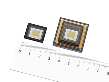
To start, Sony has created two SWIR based sensors, the IMX990 and IMX991. Both have similar characteristics and features, which are built on the Pregius™ digital sensor base providing them CMOS-like operability, functionality, and uniformity. All models are housed in a ceramic PGA package and utilize the same pin configuration thus reducing the need for multiple board designs to support both sensors. Each one can come with an optional single stage thermoelectric cooling (TEC) device to reduce dark current (heat) noise accumulation when capturing longer exposure images. The TEC has a temperature differential of ~30⁰C (at a Ta = 45⁰C).
These sensors utilize Sony’s new SenSWIR™ technology ensuring better visible \wavelength penetration and detection through a thinner surface InP (indium phosphide) layer. When this technology is combined with the Cu-Cu connection, the pixel sizes can be greatly reduced making them the industry’s smallest InGaAs based pixels, measuring just 5μm. Quantum efficiency (QE) is level and even in the visible range while being very high in the NIR range, peaking at >75% at 1,300nm. The IMX990 provides an SXGA (1280×1024), 1/2 type, resolution running at 130 fps while the IMX991 is a VGA (640×512), 1/4 Type, sensor running at 250 fps. Both sensors have a global shutter and output the image data via a 2 or 4 channel SLVS transceivers. Their smaller packages and digital transmission make them easier and quicker to implement into any new camera design.
Target Applications
Machine Vision (MV) applications have long used various different sensors to capture images at different wavelengths. In theory, this market has a lot of multi-spectral imaging applications, in practicality, but the cost of having multiple cameras and/or the higher price points of non-visible wavelength cameras make them prohibitive to use on a regular basis. It is for this reason that these new sensors are being welcomed by the MV industry. Below are some verticals that directly benefit from having one camera that can see the visible to SWIR spectrums.
Food Processing and Inspection
Bean Sorting
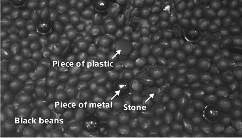
Figure 4: Bean sorting – Visible
(Image from Sony, https://www.sony-semicon.co.jp/e/products/IS/industry/technology/swir.html)
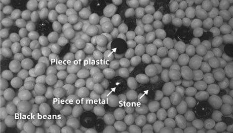
Figure 5: Bean sorting – SWIR
(Image from Sony, https://www.sony-semicon.co.jp/e/products/IS/industry/technology/swir.html)
In this vertical, contrast is key for captured images. This helps to see the defects and debris as they reflect differently than the desired product. Typically, this is done by using various colored light and/or color filters to highlight the unwanted items. The challenge happens when the foreign material has a similar reflective spectrum as the food item, typical of bean sorting. In this case, metal, stones, and plastic are not easily detectable in the visible spectrum but once you look at them in the SWIR range, they stick out making them easy to extract out of the mix
White Powder Inspection
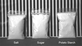
Figure 6: White powder inspection – Visible
(Image from Sony, https://www.sony-semicon.co.jp/e/products/IS/industry/technology/swir.html)
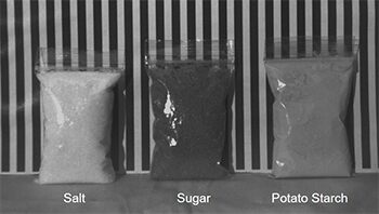
Figure 7: White powder inspection – SWIR
(Image from Sony, https://www.sony-semicon.co.jp/e/products/IS/industry/technology/swir.html)
Another challenging application is differentiating between salt, sugar, and flour. All three look very similar in RGB spectrum however have different reflectivity to SWIR light. Once these powders are subjected to this radiation and imaged with a SWIR camera, their uniqueness is easily identified and sorted
Fruit Inspection

Figure 8: Fruit inspection – Visible
(Image from Sony, https://www.sony-semicon.co.jp/e/products/IS/industry/technology/swir.html)
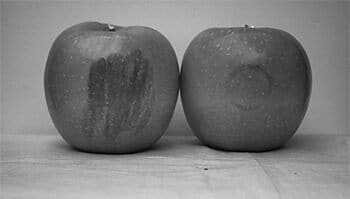
Figure 9: Fruit inspection – SWIR
(Image from Sony, https://www.sony-semicon.co.jp/e/products/IS/industry/technology/swir.html)
Another challenging application is differentiating between salt, sugar, and flour. All three look very similar in RGB spectrum however have different reflectivity to SWIR light. Once these powders are subjected to this radiation and imaged with a SWIR camera, their uniqueness is easily identified and sorted
Observation and Measuring
Temperature probe
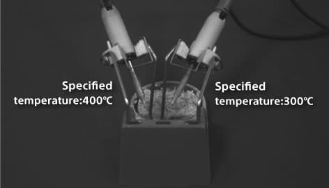
Figure 10: Temperature probe – Visible
(Image from Sony, https://www.sony-semicon.co.jp/e/products/IS/industry/technology/swir.html)
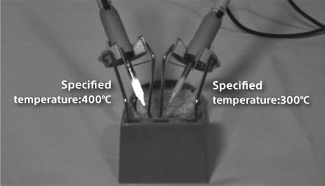
Figure 11: Temperature probe – SWIR
(Image from Sony, https://www.sony-semicon.co.jp/e/products/IS/industry/technology/swir.html)
Cameras build with Sony’s SWIR sensors have the advantage of being used to visually record temperature differences. As the SWIR range touches the thermal wavelength range, the camera can detect differences in temperature and present them as intensity values in the captured images. For example, this allows the use of cameras and machine vision applications to monitor temperature of soldering irons to determine if they have reached their ideal temperature for use
Moisture Absorption
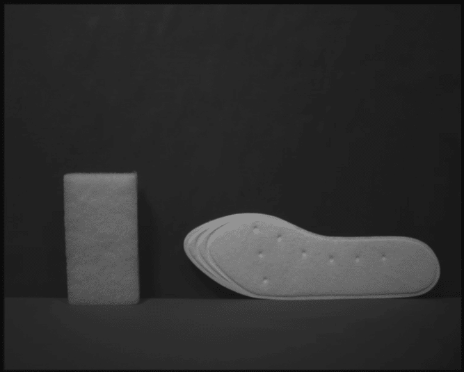
Figure 12: Moisture absorption – Visible
(Image from Sony, https://www.sony-semicon.co.jp/e/products/IS/industry/technology/swir.html)
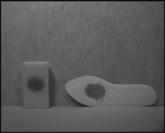
Figure 13: Moisture absorption – SWIR
(Image from Sony, https://www.sony-semicon.co.jp/e/products/IS/industry/technology/swir.html)
Water absorbs SWIR waves very well. This is an important property when checking to see if materials have penetrated or contain water. SWIR images will be darker where the moisture is present and MV algorithms can react accordingly.
With more autonomous vehicles being developed and deployed, the need to overcome environmental challenges is increasing. One of the biggest challenges with these applications is fog, mist and haze that obscures the view from the camera. SWIR wavelengths can pass through these obstructions providing better views for the navigation systems to direct the vehicle and avoid collisions with other objects
Conclusion
Many applications have benefited from leveraging a large spectrum of wavelengths to gather additional information and make assessments of a product’s quality and performance. Costs of SWIR based cameras have limited how effectively they are deployed in these verticals. With the introduction of Sony’s SenSWIR™ technology and image sensors have opened up these markets by providing a low-cost solution that spans a broad range of wavelengths. This minimizes the complexity of the vision system’s design while providing hyperspectral and multi-spectral imaging to the masses. More use cases and applications will be created as engineers evaluate cameras built with these sensors to address their needs and challenges.
About the Author


